除了设备采购外,包含英特尔在内的主要半导体业者亦达成重要协议,推动将沿用数十年的光罩标准规格从现行的6吋转型为12吋规格。这项转换虽然技术门槛与投入成本高昂,但预估可使High NA机台的产能吞吐量大幅提升40%,同时大幅简化设计流程并降低晶片制造成本,进一步缓解传统光罩尺寸对AI晶片架构与封装带来的限制。
随著台积电、三星与英特尔这三大客户全数承诺采用High NA设备并推进大尺寸光罩技术,南韩SK海力士也正评估加入联盟并规划于2028年应用。这标志著全球顶尖半导体生态系正加速迈向新一代微影制程量产,取代复杂的多重曝光技术,为未来先进AI资料中心晶片与记忆体制造奠定关键的生产基础。
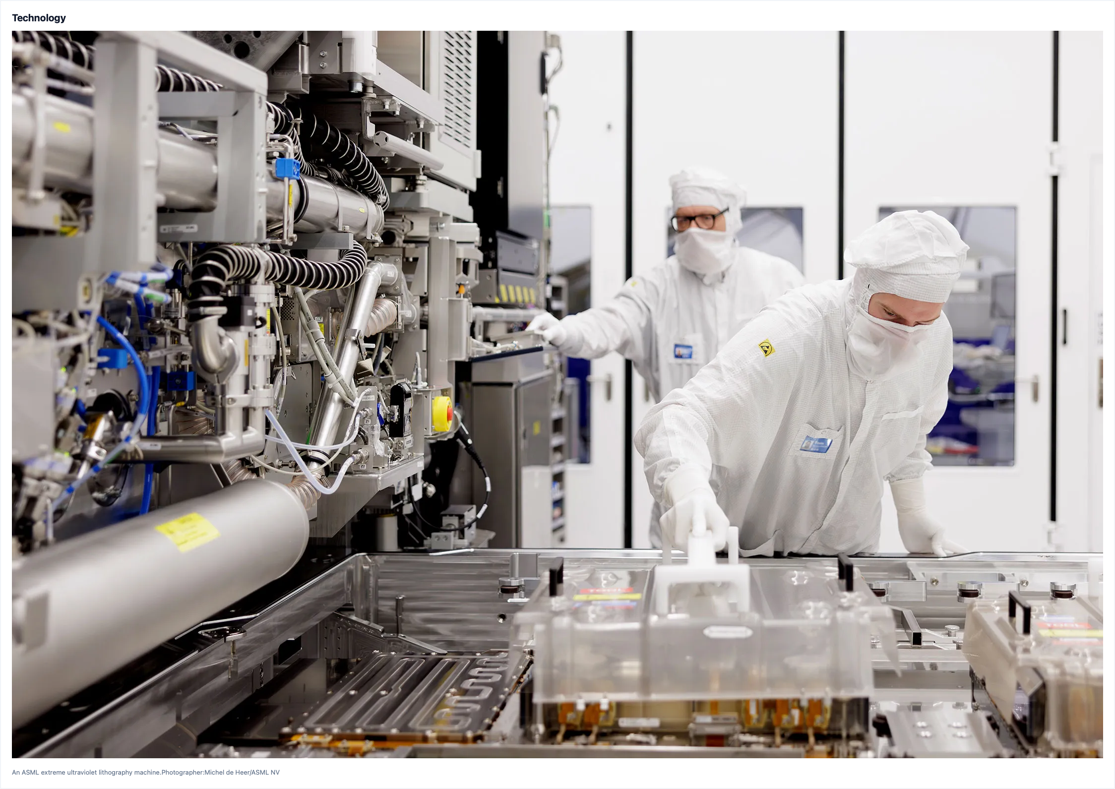
ASML Holding NV has secured major commitments from leading chipmakers, including Taiwan Semiconductor Manufacturing Co. (TSMC) and Samsung Electronics Co., to adopt its cutting-edge High NA EUV lithography equipment priced at roughly $400 million per unit to support soaring global demand for artificial intelligence hardware. Under the rollout timeline, Samsung plans to implement the technology for memory production by 2028, while TSMC aims to begin adoption for high-volume manufacturing starting in 2030.
Alongside the machinery deployment, the industry leaders—including Intel Corp.—have agreed to transition photomask technology from the conventional 6-inch format to larger 12-inch versions. Although migrating to larger masks has historically been technically demanding and costly, ASML estimates the change could increase machine throughput by 40% and streamline design processes, effectively removing architectural bottlenecks that previously forced chipmakers into complex vertical stacking and interface designs.
The unified commitment from ASML's three largest customers, accompanied by interest from SK Hynix to join the consortium and adopt High NA EUV for DRAM production by 2028, represents a critical milestone for the commercial viability of High NA lithography. This concerted shift enables manufacturers to phase out cumbersome multi-patterning approaches and establish the manufacturing infrastructure needed for next-generation AI processors and advanced memory products.