在过去的半个世纪中,芯片制造商一直通过缩小晶体管来提升性能,以符合摩尔定律。然而,平面设计正面临物理极限,晶体管出现漏电、浪费电能和成本上升的问题;彭博行业研究估计,2024年台积电N3工艺上十亿个晶体管的成本比先前的N5工艺高出约40%。为了维持技术进步,三星、IBM、英特尔和台积电等巨头正在转向垂直设计。三星和IBM近期宣布了堆叠晶体管技术,而将全环绕栅极(GAA)晶体管垂直堆叠的互补场效应晶体管(CFET)预计将在21世纪30年代初实现商用。IBM的CFET设计可将逻辑门所需面积减半,同时提升50%的性能或提高70%的能源效率。
西方公司为了突破物理限制而向垂直方向发展,而以华为为代表的中国科技巨头则是为了绕过美国的出口管制。制裁阻碍了中国企业获取阿斯麦(ASML)的极紫外(EUV)光刻机,使其难以制造微型晶体管。作为回应,华为公布了“逻辑折叠”技术,将一块芯片的电路分布在两片硅片上并面迎面精密键合。该技术大幅缩短了电信号传输的距离,从而提升了速度并将能源效率提高了40%。尽管使用较旧的制造工具,华为声称其晶体管密度达到了每平方毫米约2.38亿个,堪比台积电先进的N3工艺。
然而,三维芯片制造也带来了严重的物理挑战。散热是其中最大的瓶颈,因为三维芯片产生热量的体积增长速度快于散热表面积的增长速度。此外,现有的芯片设计软件必须彻底重构,且晶圆级键合需要极高的精度,微小缺陷就可能大幅降低良品率。因此,华为预计在2031年左右才能实现逻辑折叠芯片的大规模生产。虽然像台积电这样的竞争对手在承担垂直设计的成本之前,仍将对平面设计进行一两代迭代,但摩尔定律的放缓以及地缘政治压力正迫使整个半导体行业向上构建。
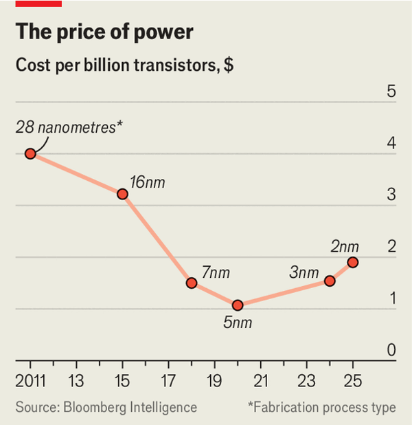
Over the past half-century, chipmakers have shrunk transistors to boost performance, conforming to Moore’s law. However, flat designs face physical limits, with transistors leaking current, wasting power, and increasing costs; Bloomberg Intelligence reports that in 2024, a billion transistors on TSMC's N3 process cost 40% more than on the N5 process. To sustain progress, giants like Samsung, IBM, Intel, and TSMC are moving towards vertical designs. Samsung and IBM recently announced stacked transistor technologies, and complementary field-effect transistors (CFETs) that stack gate-all-around (GAA) transistors are expected to emerge commercially by the early 2030s. IBM's CFET design can halve the logic gate area, boosting performance by 50% or improving energy efficiency by 70%.
While Western firms build upwards to beat the limits of physics, China’s champions, particularly Huawei, do so to bypass US export controls. Sanctions have blocked Chinese access to ASML's extreme-ultraviolet (EUV) lithography machines, preventing the manufacture of ultra-small transistors. In response, Huawei announced "Logic Folding," a method that splits a chip's circuitry across two silicon wafers and bonds them face-to-face. This technique drastically reduces the distance electrical signals must travel, increasing speed and improving energy efficiency by 40%. Despite using older equipment, Huawei claims this enables a transistor density of 238 million per square millimetre, comparable to TSMC's advanced N3 process.
However, 3D chipmaking introduces severe technical hurdles. Heat dissipation is a major bottleneck, as the heat-generating volume of 3D chips grows faster than the surface area available to cool them. Additionally, existing chip-design software must be completely rethought, and wafer-to-wafer bonding requires extreme precision where tiny defects can ruin manufacturing yields. Consequently, Huawei does not expect large-scale production of Logic Folding chips before 2031. While competitors like TSMC will continue optimizing flatter designs for another generation or two before bearing the costs of going vertical, the limits of Moore's law and geopolitical pressure are forcing the entire industry to build upwards.
Source: The future of chipmaking looks more like Manhattan than Silicon Valley
Subtitle: Constrained by physics and politics, chipmakers are building upwards
Dateline: Jul 09, 2026 06:36 AM