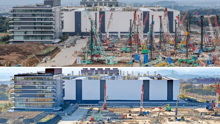
台积电考虑在日本熊本的第二座工厂改采更先进的4奈米制程,而非原先规划的6与7奈米,以因应对AI相关晶片的需求变化。该厂于10月底才开工,计划在2027年量产,但
由于自2024年宣布第二厂以来,6与7奈米晶片需求转弱,台中主力产线产能利用率不理想,加上Nvidia、Apple、Google与Amazon等客户转向更先进制程,台积电对日本扩产更趋谨慎。熊本第一厂目前生产40、28奈米以及较先进的16、12奈米晶片,主要供应工业、消费电子与车用市场。
消息人士指出,台积电已告知供应商,2026年在日本不需新增设备,并考虑将先进封装技术一并引进日本,以满足AI运算对高频宽记忆体与封装的需求。像Nvidia最新Blackwell晶片采4奈米制程并搭配CoWoS封装,Apple最新iPhone处理器则使用3奈米技术,日本厂区的最终规划仍在与包括Sony、Denso与Toyota等合作伙伴协调中。
TSMC is considering upgrading its second fab in Kumamoto, Japan from the originally planned 6- and 7-nanometer nodes to a more advanced 4-nanometer process to better serve growing AI-related demand. Construction on this plant, which started in late October and is scheduled to begin operations in 2027, has already been paused, with heavy machinery largely removed, implying potential delays and design changes.
Since TSMC announced the second Kumamoto plant in 2024, demand for 6- and 7-nanometer chips has weakened and utilization at its main Taichung lines has become unsatisfactory, as major customers like Nvidia, Apple, Google, and Amazon shift to more cutting-edge nodes. The first Kumamoto fab currently produces 40- and 28-nanometer chips and more advanced 16- and 12-nanometer products for industrial, consumer electronics, and automotive uses, but TSMC has told suppliers it will not need additional equipment in Japan through all of 2026.
Sources say TSMC is also weighing bringing its advanced packaging technologies, such as those used in AI accelerators, to Japan, given the importance of high-bandwidth memory and sophisticated packaging for AI computing. Nvidia’s latest Blackwell chip uses TSMC’s 4-nanometer process and CoWoS packaging, while Apple’s newest iPhone processors rely on 3-nanometer technology, and the final configuration of Japan Advanced Semiconductor Manufacturing, backed by Sony, Denso, and Toyota, remains under negotiation even as TSMC insists its Japan projects are proceeding.